- 您现在的位置:买卖IC网 > Sheet目录327 > HW-V4-ML410-UNI-G-J (Xilinx Inc)EVALUATION PLATFORM VIRTEX-4
Chapter 2: ML410 Embedded Development Platform
R
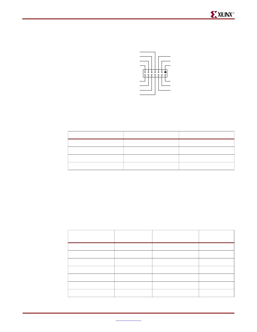
The pinout shown in Figure 2-12 is compatible with the Parallel Cable IV (PC4) JTAG
programming solution. The J9 header is used when programming the FPGA by way of the
PC4 download cable.
GND
GND
GND
GND
GND
GND
1 3
1
GND
J9
INIT
NC
PC4_TDI
S Y S ACE_TDO
14
2
VCC 3 V 3
PC4_TM S
PC4_TCK
UG0 8 5_12_111505
Figure 2-12:
PC4 JTAG Connector Pinout (J9)
The JTAG configuration port on the System ACE CF controller is connected directly to the
Table 2-14:
JTAG Connection from System ACE CF to FPGA
Signal Name
FPGA_TCK
FPGA_TDO
FPGA_TDI
FPGA_TMS
System ACE Pin (U38)
80
81
82
85
FPGA Pin (U37)
AA14
W17
AA15
Y14
Non-Volatile Storage through the MPU Interface
In addition to programming the FPGA and storing bitstreams, the System ACE CF
controller can be used to facilitate general-use, non-volatile storage. The System ACE CF
controller provides an MPU interface for allowing a microprocessor to access the
CompactFlash memory, enabling the use of the CompactFlash card as a file system. The
System ACE MPU interface is capable of supporting 16-bit or 8-bit modes of operation
because all 16 data lines are wired to the FPGA.
Table 2-15:
System ACE MPU Connection from FPGA to Controller
UCF Signal Name
SYSACE_FPGA_CLK
SYSACE_CLK_OE
SYSACE_MPA[0]
SYSACE_MPA[1]
SYSACE_MPA[2]
SYSACE_MPA[3]
SYSACE_MPA[4]
FPGA Pin
(U37)
AF16
AD4
AE6
AE4
AE3
AF6
AF5
Schematic Signal Name
SYSACE_FPGA_CLK
SYSACE_CLK_OE
SYSACE_MPA[00]
SYSACE_MPA[01]
SYSACE_MPA[02]
SYSACE_MPA[03]
SYSACE_MPA[04]
System ACE Pin
(U38)
93
77
70
69
68
67
45
46
ML410 Embedded Development Platform
UG085 (v1.7.2) December 11, 2008
发布紧急采购,3分钟左右您将得到回复。
相关PDF资料
HW-V5-ML501-UNI-G
EVALUATION PLATFORM VIRTEX-5
HW-V5-ML507-UNI-G
EVAL PLATFORM V5 FXT
HW-V5-ML550-UNI-G
EVALUATION PLATFORM VIRTEX-5
HW-V5-ML555-G
BOARD EVAL FOR VIRTEX-5 ML555
HW-V5-ML561-UNI-G
EVALUATION PLATFORM VIRTEX-5
I-JET
JTAG ARM DEBUGGING PROBE
IAC24A
INPUT MODULE AC 5MA 24VDC
IAC5EQ
INPUT MODULE AC 10MA 5VDC
相关代理商/技术参数
HW-V4-ML423-UNI-G
功能描述:EVALUATION PLATFORM VIRTEX-4 RoHS:是 类别:编程器,开发系统 >> 过时/停产零件编号 系列:Virtex®-4 标准包装:1 系列:- 传感器类型:CMOS 成像,彩色(RGB) 传感范围:WVGA 接口:I²C 灵敏度:60 fps 电源电压:5.7 V ~ 6.3 V 嵌入式:否 已供物品:成像器板 已用 IC / 零件:KAC-00401 相关产品:4H2099-ND - SENSOR IMAGE WVGA COLOR 48-PQFP4H2094-ND - SENSOR IMAGE WVGA MONO 48-PQFP
HW-V4-ML423-UNI-G-J
功能描述:EVALUATION PLATFORM VIRTEX-4 RoHS:是 类别:编程器,开发系统 >> 通用嵌入式开发板和套件(MCU、DSP、FPGA、CPLD等) 系列:Virtex®-4 产品培训模块:Blackfin® Processor Core Architecture Overview
Blackfin® Device Drivers
Blackfin® Optimizations for Performance and Power Consumption
Blackfin® System Services 特色产品:Blackfin? BF50x Series Processors 标准包装:1 系列:Blackfin® 类型:DSP 适用于相关产品:ADSP-BF548 所含物品:板,软件,4x4 键盘,光学拨轮,QVGA 触摸屏 LCD 和 40G 硬盘 配用:ADZS-BFBLUET-EZEXT-ND - EZ-EXTENDER DAUGHTERBOARDADZS-BFLLCD-EZEXT-ND - BOARD EXT LANDSCAP LCD INTERFACE 相关产品:ADSP-BF542BBCZ-4A-ND - IC DSP 16BIT 400MHZ 400CSBGAADSP-BF544MBBCZ-5M-ND - IC DSP 16BIT 533MHZ MDDR 400CBGAADSP-BF542MBBCZ-5M-ND - IC DSP 16BIT 533MHZ MDDR 400CBGAADSP-BF542KBCZ-6A-ND - IC DSP 16BIT 600MHZ 400CSBGAADSP-BF547MBBCZ-5M-ND - IC DSP 16BIT 533MHZ MDDR 400CBGAADSP-BF548BBCZ-5A-ND - IC DSP 16BIT 533MHZ 400CSBGAADSP-BF547BBCZ-5A-ND - IC DSP 16BIT 533MHZ 400CSBGAADSP-BF544BBCZ-5A-ND - IC DSP 16BIT 533MHZ 400CSBGAADSP-BF542BBCZ-5A-ND - IC DSP 16BIT 533MHZ 400CSBGA
HW-V4SX35-VIDEO-SK-EC
功能描述:VIRTEX-4 VIDEO STARTER KIT RoHS:否 类别:编程器,开发系统 >> 过时/停产零件编号 系列:Virtex®-4 标准包装:1 系列:- 传感器类型:CMOS 成像,彩色(RGB) 传感范围:WVGA 接口:I²C 灵敏度:60 fps 电源电压:5.7 V ~ 6.3 V 嵌入式:否 已供物品:成像器板 已用 IC / 零件:KAC-00401 相关产品:4H2099-ND - SENSOR IMAGE WVGA COLOR 48-PQFP4H2094-ND - SENSOR IMAGE WVGA MONO 48-PQFP
HW-V4SX35-VIDEO-SK-UK
功能描述:VIRTEX-4 VIDEO STARTER KIT RoHS:否 类别:编程器,开发系统 >> 过时/停产零件编号 系列:Virtex®-4 标准包装:1 系列:- 传感器类型:CMOS 成像,彩色(RGB) 传感范围:WVGA 接口:I²C 灵敏度:60 fps 电源电压:5.7 V ~ 6.3 V 嵌入式:否 已供物品:成像器板 已用 IC / 零件:KAC-00401 相关产品:4H2099-ND - SENSOR IMAGE WVGA COLOR 48-PQFP4H2094-ND - SENSOR IMAGE WVGA MONO 48-PQFP
HW-V5GBE-DK-UNI-G
功能描述:KIT DEV V5 LXT GIGABIT ETHERNET RoHS:是 类别:编程器,开发系统 >> 通用嵌入式开发板和套件(MCU、DSP、FPGA、CPLD等) 系列:Virtex®-5 LXT 产品培训模块:Blackfin® Processor Core Architecture Overview
Blackfin® Device Drivers
Blackfin® Optimizations for Performance and Power Consumption
Blackfin® System Services 特色产品:Blackfin? BF50x Series Processors 标准包装:1 系列:Blackfin® 类型:DSP 适用于相关产品:ADSP-BF548 所含物品:板,软件,4x4 键盘,光学拨轮,QVGA 触摸屏 LCD 和 40G 硬盘 配用:ADZS-BFBLUET-EZEXT-ND - EZ-EXTENDER DAUGHTERBOARDADZS-BFLLCD-EZEXT-ND - BOARD EXT LANDSCAP LCD INTERFACE 相关产品:ADSP-BF542BBCZ-4A-ND - IC DSP 16BIT 400MHZ 400CSBGAADSP-BF544MBBCZ-5M-ND - IC DSP 16BIT 533MHZ MDDR 400CBGAADSP-BF542MBBCZ-5M-ND - IC DSP 16BIT 533MHZ MDDR 400CBGAADSP-BF542KBCZ-6A-ND - IC DSP 16BIT 600MHZ 400CSBGAADSP-BF547MBBCZ-5M-ND - IC DSP 16BIT 533MHZ MDDR 400CBGAADSP-BF548BBCZ-5A-ND - IC DSP 16BIT 533MHZ 400CSBGAADSP-BF547BBCZ-5A-ND - IC DSP 16BIT 533MHZ 400CSBGAADSP-BF544BBCZ-5A-ND - IC DSP 16BIT 533MHZ 400CSBGAADSP-BF542BBCZ-5A-ND - IC DSP 16BIT 533MHZ 400CSBGA
HW-V5GBE-DK-UNI-G-J
功能描述:KIT DEV GIGABIT ETHERNET VIRTEX5 RoHS:是 类别:编程器,开发系统 >> 通用嵌入式开发板和套件(MCU、DSP、FPGA、CPLD等) 系列:Virtex®-5 LXT 产品培训模块:Blackfin® Processor Core Architecture Overview
Blackfin® Device Drivers
Blackfin® Optimizations for Performance and Power Consumption
Blackfin® System Services 特色产品:Blackfin? BF50x Series Processors 标准包装:1 系列:Blackfin® 类型:DSP 适用于相关产品:ADSP-BF548 所含物品:板,软件,4x4 键盘,光学拨轮,QVGA 触摸屏 LCD 和 40G 硬盘 配用:ADZS-BFBLUET-EZEXT-ND - EZ-EXTENDER DAUGHTERBOARDADZS-BFLLCD-EZEXT-ND - BOARD EXT LANDSCAP LCD INTERFACE 相关产品:ADSP-BF542BBCZ-4A-ND - IC DSP 16BIT 400MHZ 400CSBGAADSP-BF544MBBCZ-5M-ND - IC DSP 16BIT 533MHZ MDDR 400CBGAADSP-BF542MBBCZ-5M-ND - IC DSP 16BIT 533MHZ MDDR 400CBGAADSP-BF542KBCZ-6A-ND - IC DSP 16BIT 600MHZ 400CSBGAADSP-BF547MBBCZ-5M-ND - IC DSP 16BIT 533MHZ MDDR 400CBGAADSP-BF548BBCZ-5A-ND - IC DSP 16BIT 533MHZ 400CSBGAADSP-BF547BBCZ-5A-ND - IC DSP 16BIT 533MHZ 400CSBGAADSP-BF544BBCZ-5A-ND - IC DSP 16BIT 533MHZ 400CSBGAADSP-BF542BBCZ-5A-ND - IC DSP 16BIT 533MHZ 400CSBGA
HW-V5GBE-DK-UNI-G-PROMO1
功能描述:KIT DEV V5 LXT GIGABIT ETHERNET RoHS:是 类别:编程器,开发系统 >> 过时/停产零件编号 系列:- 标准包装:1 系列:- 传感器类型:CMOS 成像,彩色(RGB) 传感范围:WVGA 接口:I²C 灵敏度:60 fps 电源电压:5.7 V ~ 6.3 V 嵌入式:否 已供物品:成像器板 已用 IC / 零件:KAC-00401 相关产品:4H2099-ND - SENSOR IMAGE WVGA COLOR 48-PQFP4H2094-ND - SENSOR IMAGE WVGA MONO 48-PQFP
HW-V5GBE-DK-UNI-G-PROMO2
功能描述:KIT DEV V5 LXT GIGABIT ETHERNET RoHS:是 类别:编程器,开发系统 >> 过时/停产零件编号 系列:Virtex® 标准包装:1 系列:- 传感器类型:CMOS 成像,彩色(RGB) 传感范围:WVGA 接口:I²C 灵敏度:60 fps 电源电压:5.7 V ~ 6.3 V 嵌入式:否 已供物品:成像器板 已用 IC / 零件:KAC-00401 相关产品:4H2099-ND - SENSOR IMAGE WVGA COLOR 48-PQFP4H2094-ND - SENSOR IMAGE WVGA MONO 48-PQFP
